Lab #6
Non-Ideal Transistors
Real transistors are devices which depart from the ideal components assumed previously. This lab explores the Ebers-Moll model, intrinsic emitter resistance, temperature effects, and the Early effect.
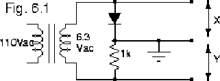
1) Turn your scope into an I-V curve tracer, and measure the I-V curve of a diode, as seen in Fig. 6.1. Put the scope in X-Y mode to plot V across the diode vs. V across the 1kΩ resistor (and thus, the current). Use a 1N4148 or 1N914 signal diode. Find where the zero points are for each axis, and what the X and Y scales on the scope equate to in actual V and I. Reverse the polarity of the diode. Note the slope of the forward diode curve. Vdiode/Idiode
should be around 100mV/decade. Make quantitative sketches of all the I-V curves you measure today, and relish the fact that you don't have to take data points and plot them yourself as you did in previous labs.
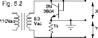
2) Use a 2N3904 transistor instead of the diode (Fig. 6.2) and trace its IE vs. VBE. We care more about IC vs. VBE - why is the measurement we're making useful? Why do we do it this way? Can you observe the breakdown voltage for the BE junction? Prevent the breakdown by installing a protection diode between the base and ground. Include a schematic of this new circuit. What is the slope of the transistor's curve? (hopefully around 60mV/decade).
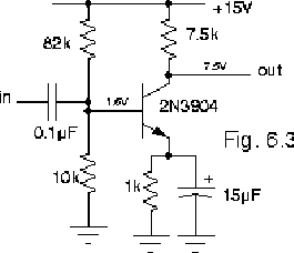
3) Make the grounded emitter amplifier shown in Fig. 6.3. If the exact components in this schematic aren't in your toolkit, choose alternate valued resistors and capacitors. Explain how you chose these alternate values, and predict any remaining differences between the behavior of the circuit in the schematic and the circuit you actually built. Check the quiescent collector voltage. Then drive it with a small triangle wave at 10kHz, at the largest amplitude which does not produce clipping. You might have to build a voltage divider to make the input signal small enough for this. Sketch the shape distortion which the text calls “barn roof distortion”, and explain why this occurs. Remove the 15F capacitor, increase the input amplitude, measure the voltage gain, and compare to your prediction. Put the capacitor back and reduce the amplitude of the input signal as much as possible. Predict the gain at the quiescent point using re. Measure it and compare.
4) Build the current mirror shown in Fig. 6.4. Note that these are PNP transistors, so the signs are reversed from the other transistors you have used. Compare the program current (calculate what this is) and the output current - do they match? There are two effects working here - temperature differences between the two transistors changing their respective Ebers-Moll equations, and the Early effect. Change the temperatures of the two transistors with your fingers and observe the change in the output current. Explain why Iout changes as it does with the temperature changes.

Add 100Ω emitter resistors to each transistor. Draw the new schematic, letting things cool off while you do so. Now check Iout compared to the program current. Use your fingers to heat the elements again and record the current differences. Compare to the first circuit. These resistors provide negative feedback to the transistors. As Ic grows due to temperature changes and/or the Early effect, Ohm's law says the voltage drop across the emitter resistor also grows, raising VE and thus lowering VBE and Ic.