Lab #12:
Fiddling with Flip-Flops
This lab will introduce a variety of flip-flops and includes the construction of a simple binary counter from JK flip-flops. It is important to remember that flip-flops are the foundation of sequential logic systems and in recording lab work the precise order of input states you follow is important in determining the output at each stage of the measurement. Keep careful notes of your measurements for use in writing your lab report.
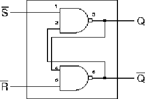
1) Build a basic SR (set-reset) flip-flop (FF) using simple TTL gates (74LS00 NAND gates). Determine its behavior completely by measuring its truth table for all possible inputs as well as initial output states. Be very careful to completely specify the sequence of inputs you try. Remember, the behavior of the outputs depends not only on the present inputs but also the history of input states leading up to the present. Are the inputs active high or low and what does this mean? Does the circuit behave as described in class?
2) Now add clocking to the basic SR FF. This requires a couple more gates and changes the level at which the inputs are active. First try using a manual clock input, i.e. just a wire you switch between ground and 5V. Again measure the truth table, first with the clock low and then with the clock high, in order to verify that the flip-flop pays attention to the S and R inputs only when the clock is high. Then automate the clock by using the function generator. The SYNC signal is compatible with TTL levels - verify this by examining the SYNC with the scope before using it as an input to a TTL gate - recall TTL's immense dislike of voltages outside the specified limits of 0 to 5 volts. This provides an easily adjustable clock pulse rate. You could make the normal output of the function generator TTL compatible by using the amplitude and offset controls, but you would then run the risk of bumping the controls and toasting your gates. This sort of accident can't happen with the SYNC output. With the clock set to a slow rate, determine when in the clock cycle (high, low, rising edge, falling edge) the change in the output occurs. Do this by displaying both the CLK input and the Q output on the scope simultaneously and playing with the inputs after the clock has gone low or high. Use a low frequency for the clock, slow down the horizontal sweep on the scope, and hook up easily switched inputs so you can more easily control your measurements.
3) Now turn the circuit into a D-type latch as shown. Verify that it does, in fact, latch input data when the clock is high and remember that data when the clock is low. The necessary inverter can be produced from a NAND gate or you can use one from a 74LS04.
4) Now for a real flip-flop. Try a 74LS107A IC, a dual JK flip-flop with clear. Examine its pinout on the data sheet. Keeping the CLR input high, examine the behavior of the device and determine its truth table. Ascertain when in the clock cycle the outputs change state in the same way as you did with the simple FF in part #2. Make measurements to verify that this is indeed an edge-triggered device, not merely a level-sensitive master-slave configuration which updates the outputs on the clock's falling edge. Determine the function of the CLR input. Does the CLK input affect the CLR input? Is CLR active high or low? This chip will be the basis for building a timer.